Element Structure of UV-C LED
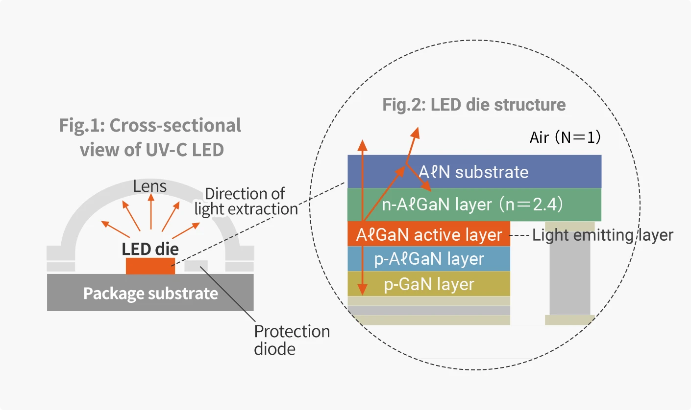
Structure of UV-C LED
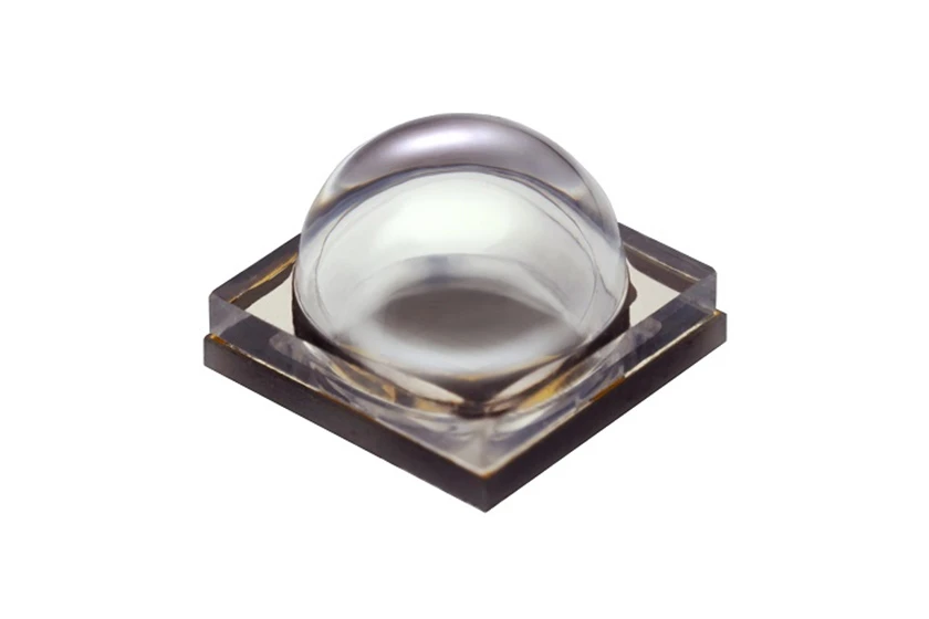
A UV-C LED consists of the LED die, protection diode, package substrate, and a lens.

The three technologies that achieve high quality, high output and high efficiency
Stanley Electric developed a proprietary UV-C LED not achievable by other companies by seeking ways to improve the LED die and package structure.
LED Die
As shown in [Fig.2], the LED die is made by stacking each layer on the AℓN substrate at the very top. Stanley Electric uses two distinctive techniques for the AℓN substrate, which is the foundation of these stacked layers.
Using Substrate Material with Few Crystal Defects
The substrate, which forms the groundwork for the LED die structure, is the part that acts as the foundation to stack the layers. If the lattice constant (spacing between crystal grains) difference of the substrate and n-AℓGaN (aluminum gallium nitride) layer is large, crystal defects will increase. Therefore, using a substrate with material that is similar to the n-AℓGaN layer improves the crystal quality.
Sapphire material used for blue LEDs is used in many UV-C LED substrates. However, since the crystal grain spacing (lattice constant) is large, cracks easily form in the substrate stacked layer and stacking layers for short wavelengths such as 265 nm is especially difficult. When cracks form, it is not possible to emit light efficiently even when using a large current. Furthermore, the substrate temperature will rise when just using a small current resulting in a drop in efficiency.
| Type of die | Structure | Features |
|---|---|---|
| AℓN substrate | Crystal defects→10 thousand/cm2 1/10,000 of sapphire substrate Few crystal defects |
◎
High efficiency High output |
| Sapphire substrate |
Crystal defects→100 million/cm2 Many crystal defects |
×
Low efficiency Low output |
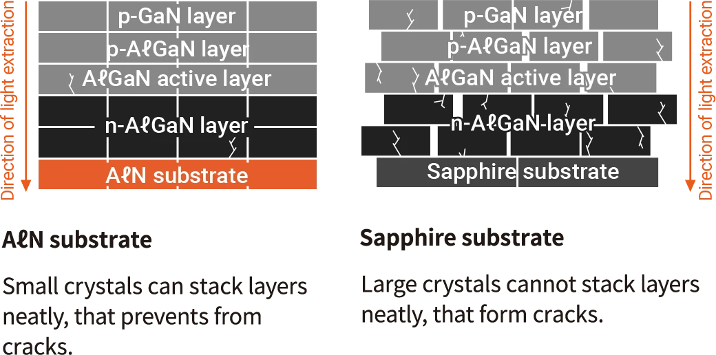
Stanley Electric has acquired HexaTech, Inc., which owns AIN substrates consisting of aluminum(Aℓ) and nitrogen(N), to possess AℓN substrate manufacturing that requires advanced technical capabilities in order to achieve the 265 nm wavelength with high disinfection efficiency. Since we were able to create a well-formed stacked layer structure with a small crystal grain spacing [See Fig.3] this resulted in making it difficult to form cracks (few crystal defects).
Fig.3: Laminated Structure Comparison
This enables light to be generated at a low current and with high output. Stanley's LEDs can maintain high output even at high currents.
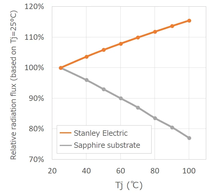
Furthermore, the use of AℓN substrates with few crystal defects achieves high output even in high temperature environments. The efficiency of competitor LEDs drops significantly when the temperature rises but Stanley Electric's LED can maintain high efficiency and has superior temperature characteristics [See Fig.4].
Fig.4: Comparison of Temperature Characteristics by Substrate Material
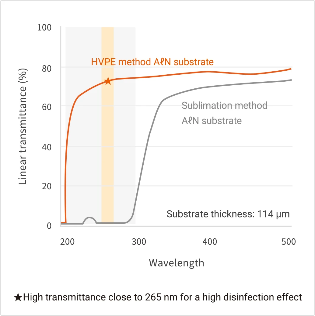
Creation Method to Achieve a Stacked Layer Substrate with High Transmittance Regardless of the Width
This technology is to extract light emitted from the die (light extraction efficiency). AℓN substrates is a kind of window for the LED die and the greater the transparency, the more bright light can be extracted. Also, using thicker substrates leads to a decrease in the difficulty of handling them during the manufacturing process. Meaning that high transparency and thickness are both important factors for the substrate. However, with the standard sublimation method, impurities enter the crystal causing reduced transparency and when attempting to make the substrate thicker, it will unfortunately reduce the transparency. This is why Stanley Electric adopted a technology referred to as the HVPE (Hydride Vapor Phase Epitaxy) method to create a highly transparent substrate that still retains its thickness. In comparison to AℓN substrates based on the conventional sublimation method, transmittance is remarkably higher for wavelengths of 300 nm or less (close to 265 nm for a high disinfection effect) and this enables light to be efficiently extracted [See Fig.5]. This achieves high efficiency by extracting light strongly emitted from the device with greater efficiency.
Fig.5: Transmittance Characteristics of AℓN Stacked Layer Substrate Created Using the HVPE Method
Related Information
-
Light Source Technology
-
Water Disinfection
-

Surface and Air Disinfection